![[Photo of the Author]](../../common/images/Guido-S.gif)
by Guido Socher (homepage)
About the author:
Guido likes Linux because it is a really good system to
develop your own hardware.
Content:
|
A digital DC powersupply
![[Illustration]](../../common/images2/article379/title_379.jpg)
Abstract:
A very important device for hobby electronic is a
reliable DC powersupply. A proper electronically stabilized
powersupply can easily cost over 150 Euro.
Using a clever microcontroller based design we can build a power
supply which has more features and is a lot cheaper.
Those readers who are new to this series should first read
Programming the AVR microcontroller with
GCC.
Don't worry if the printed circuit board looks like it is too complicated
for your home lab. All parts and a properly etched PCBs will again
be available from
shop.tuxgraphics.org.
_________________ _________________ _________________
|
Introduction
In 2002 I wrote a linuxfocus.org article about a Microcontroller based
DC powersupply (LF
November2002 article251)
The article received a lot of interest as I noticed from emails which
I received on this subject. The design of this powersupply was however
something for advanced hobby electronic fans due to the complexity of the
circuit.
So here is now a new design which is less complex but has a lot more
features.
- Only cheap and standard components are used.
- Only one power source is needed (no separate negative supply voltage for operational
amplifiers)
- The display shows pre-set and actual values for voltage and current at the
same time.
- You can completely control the powersupply via your PC or you can use it
standalone.
- It is very small and very powerful.
How was it possible to remove components and add more features? The trick is to
move functionality which was previously based on analog components like operational
amplifiers into the microcontroller. In other words the complexity of the
software and algorithms is higher but hardware complexity is reduced. This
reduces the overall complexity for you as the software can just be copied.
It has also helped that the Atmega8 can do much more than the now phased out
AT90S4433 microcontroller.
In this article you will also learn new things about the Atmega8. You have seen
how to use the analog to digital converter. Now we will add a very fast
digital to analog converter which can be useful for a lot of other circuits.
In this article we will discuss the hardware and electrical design. There will
then be two more articles where I explain the software. We will also gradually
add more features. However adding those will require only software changes.
The basic electrical design idea
I could of course give you just the circuit diagram and some instructions on how
to build it. It will probably work but you will not know how it works. Most
hobby electronic kits are like that.
The idea of the shop.tuxgraphics.org
online shop is however to provide good and free documentation together with the
development kits. In the documentation (e.g this article) we explain really how
things work and why it was designed that way. I find it much more fun to build
something that I understand and I hope you like it too.
Let's start with the simplest possible electronically stabilized powersupply.
It consists of 2 basic parts: a transistor and a reference voltage generated
with a Z-diode.
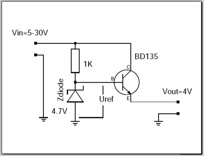
The output voltage of this circuit is Uref - 0.7V. The 0.7V are approximately
the voltage drop you get between B and E on the transistor. The Z-diode and
the resistor generate a reference voltage which is stable, even if the input
fluctuates and is noisy. The transistor is needed to handle higher currents
than the Z-diode and resistor alone can provide. In this configuration the
transistor just amplifies the current. The current which the resistor and
Z-diode need to provide is output current divided by hfe (hef is a number
which you can lookup in the datasheet of the transistor).
What are the problems with this circuit?
- The transistor will die when there is a short circuit on the output.
- It provides only a fixed output voltage.
These are quite severe limitations which make this circuit unusable but this
circuit is
still the basic building block of all electronically regulated power supplies.
To overcome those problems you need
some "intelligence" which will regulate the
current on the output and a variable reference voltage. That's all (... and
this makes the circuit much more complex).
For the last few decades people have used operational amplifiers to provide this
intelligence. Operational amplifiers can basically be used as analog calculators to
add, subtract, multiply or logically "or" voltages and currents.
Today microcontrollers are so fast that all this can easily be done in software.
The beauty is that you get as a side effect a voltmeter and an amperemeter
for free. The control loop in the microcontrollers has to know voltage and
current values anyhow. You just need to display it.
What we need from the microcontroller are:
- A AD-converter to measure voltage
and current all the time
- A DA-converter to send commands to our power transistor (provide the
reference voltage)
The problem is that DA-converter needs to be very fast. If there is a short
circuit detected on the output then we must immediately reduce the voltage
on the Basis of the transistor otherwise it will die. Fast means within
milliseconds (as fast as an operational amplifier).
The Atmega8 has an AD-converter which is more than fast enough but it has
at first glance no DA-converter. It is possible to use pulse width modulation
and an analog low pass filter to get an DA-converter but this is much too slow
to implement the short circuit protection in software. How to build a fast
DA-converter?
The R-2R ladder
There are many ways to build a digital to analog converter but we need a
fast and cheap one which can easily interface to our microcontroller.
There is a DA-converter circuit known as "R-2R ladder". It consists of resistors
and switches only. There are two types of resistors. One with R and one
with twice the value of R.
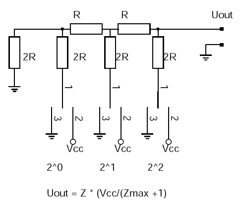
The above shows a 3 bit R2R-DA-converter. The control logic moves the switches
between GND and Vcc. A digital "1" connects the switch to Vcc and a digital
"zero"
to GND. What does this circuit do? It provides voltages in steps of Vcc/8.
In general the output voltage is Z * (Vcc/(Zmax+1) where Z is the digital
number. In the case of a 3 bit AD converter this is: 0-7.
The inner resistance of the circuit as seen from the output is R.
Instead of using separate switches we can connect the R-2R ladder to the
microcontroller output lines. A output pin of the atmega8 can provide
about 10mA but at this current you notice already a voltage drop. We would
like to use the full output range from 0-5V so the load on the output should
be less than 1mA. In other words we build a R-2R ladder with 5K and 10K
resistors.
The AD-converter of the Atmega8 has a resolution of 10bit. To use the resolution
completely we need also 10bit for the DA-converter. In other words we need to
find 10 output pins which are not used by anything else. This is a little
challenge as we would also like to have a keyboard, LCD display and I2C serial
interface to the PC but the Atmega8 is quite good. It just fits.
A more detailed design
So here is now a more detailed design of the above circuit.
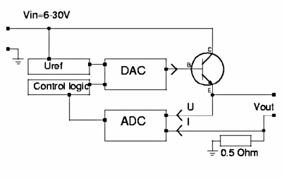
I don't want to
disappoint you but it is unfortunately still a circuit which will not be usable.
However it very good to understand the idea which is behind the final circuit.
So what is wrong with this circuit? There are mainly two things:
- The DAC (digital to analog converter) can not provide the current to drive
the power transistor
- The microcontroller operates at 5V so the maximum output of the DAC is 5V
which means that the maximum output voltage behind the power transistor will be
5-0.7=4.3V .
To fix this we must add amplifiers for current and voltage.
The final circuit
When adding amplifiers we must keep in mind that those must work with large
signals. Most amplifier design (e.g for audio) is done under the assumption
that the signals will be small compared to the supply voltage. So forget all the
classic books about transistor amplifier design.
We could use operational amplifiers but those would require extra positive and
negative supply voltages which we want to avoid.
There is also the additional requirement that the amplifier must go from zero
supply voltage to a stable state without generating any output peek. In other
words there must not be any short oscillation or output peek when you switch
on the powersupply.
What to do? Well this is not an easy task at all and requires some experience.
I will go with you through the final circuit and do the needed calculations.
We start with the power transistor. According to the datasheet the BD245B has
a hfe=20 at 3A output. It will therefore draw about 150mA on the Basis.
To amplify the current (reduce the current needed to drive the circuit) we use
a configuration known as "Darlington transistor". For this we put a BD137
in front. It has a hfe value of 50-100. This will reduce the current needed to
less than 3mA (150mA / 50).
3mA are manageable with small signal transistors like BC547/BC557. Those
small signal transistors are then very good for building a voltage amplifier.
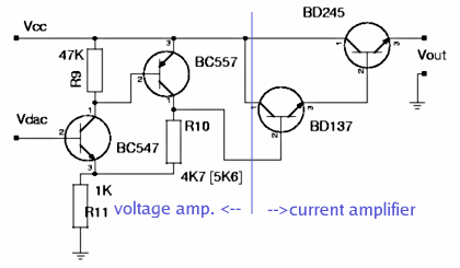
For 30V output we must at least amplify the 5V from the DAC by a factor of 6.
For this we combine a PNP and an NPN transistor as shown below. The voltage amplification
factor of this circuit is:
Vampl= (R10 + R11)/R11
The powersupply shall be
available in 2 version: Max 30 output and max 22V output. A combination of 1K
and 5.6K gives a factor of 6.6 which is good for the 30V version. For the 22V
version we use 1K and 4.7K.
The inner resistance of the circuit as seen on the Basis of BC547 is:
Rin=hfe1 * S1 * R11 * R9 = 100 * 50 * 1K * 47K = 235 MOhm

- hfe is about 100 to 200 for a BC547 transistor
- S is the slope of the amplification curve of a transistor and is
 about 50 [unit=1/Ohm]
This is more than high enough for the connection to our DAC which has a inner resistance of 5K.
The inner equivalent output resistance is:
Rout= (R10 + R11) / (S1 + S2 * R9 * R11) = about 2 Ohm
Low enough to drive the following BD137.
R9 ties Basis of BC557 to
Emitter which means "off" for the transistor until the DAC and BC547 come up.
R11 and R10 tie the Basis of BD137 initially to ground which shuts the output
Darlington stage down.
In other words every component in this amplifier stage is initially off.
This means we will not get from those transistors any oscillations or output
peeks at power on.
Now you have seen how such a circuit is designed. We need to add some
protection diodes and capacitors to stabilize the circuit and we are done.
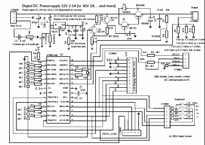
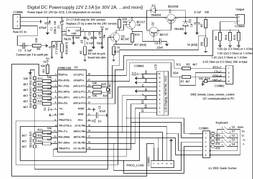
The final circuit in big as:
[PNG]
[PDF]
The values in square brackets are for the 30V version.
The circuit diagram and the board layout file (pcb format) are also
included in the tar.gz package which you can download at the end of
this article.
The connector called "Raw DC in" (=CONN6) has 3 pins. Pin 1 is "plus" pin 2 is
"minus" (=GND) and pin 3 should be connected to the earth pin. In other words
"earth" is neither directly connected to GND nor to "plus".
The limits
From previous experience I know that most readers would like to
"customize" the circuit a bit. Here is a list of hardware limits
and how to overcome them:
78L05: max input voltage 30V, the ZD8.2 extends this limit
       to about 38V. Using a different Z-diode you can extend this
       a bit. I would not go beyond 45V.
       The max output voltage should be at least 2V lower than
       the input voltage.

BD245B: 10A 80W, The 80W are however at a temperature of 25'C
        In other words add a safety margin and calculate with 60W-70W:
        (Max input voltage * Max current) < 70W

        You can add a second BD245B to go up to 120W. To ensure
        that the current distributes equally add a 0.22 Ohm resistor
        into the Emitter line of each BD245B.
        The same circuit and board can be used. Mount the transistors
        on a proper aluminum cooler and connect them with short
        wires to the board.

Current measurement shunt:
        This is a 0.5 or 0.55 Ohm resistor with 6W. This is good enough
        for about 3A of output (Iout^2 * 0.55 <= 6W). Use a resistor
        with more watts for higher currents.
Power sources
You can either use a transformer, rectifier and big capacitors or
you can try to get a 32/24V laptop powersupply.
I went for the later option. Those laptop powersupply "bricks" are
sometimes sold very cheap (over stock) and some of them provide
70W at 24V or even 32V DC.
Most people will probably go for a transformer because those are
very easy to get.
22V 2.5A version:  you need a 18V 2.5A transformer, a rectifier
                   and a 3000uF capacitor. (reason: 18 * 1.4 = 25V,
                                            at least 1000uF per ampere)

30V 2A version:    you need a 24V 2A transformer, a rectifier and
                   a 2200uF capacitor. (reason: 24 * 1.4 = 33.6V,
                                        at least 1000uF per ampere)

It does not harm to buy a transformer which can provide more ampere.

A power diodes bridge with 4 diodes which are specified for a
low volatage drop (e.g BYV29-500) gives a good
rectifier.
Note that the above dimensioning is not meant for permanent maximum
power output (reason: 22*2.5 > 18*2.5). There is no problem to use
the maximum power for 10-20min. The transformer will get a bit warm
but that is only for a short time. If you want max power output not only
for peak current but over hours and days then limit the max output
current or voltage in the hardware_settings.h file.
You can also
use a "heavier" transformer but be aware that the upper limit is
given by the power transistor. Formula:
VotageOfTransformer * 1.4 * MaxCurrent < 70W
The 70W is Ptot of BD245 minus 10W savety margin.
Check your circuit for proper insulation. Make sure that it is not possible to
touch any part that may carry 110V/230V even when the case it open.
Connect all metal parts of the chassis to earth (not to GND of the circuit).
Testing
When you have soldered everything together then do not insert the
microcontroller into the socket yet. Do some basic tests first.
Test1:
Connect some powersupply (at least 15V) to the power input of the circuit and
check that you get 5V DC behind the voltage regulator.
Test2: Measure the output voltage. It should be 0V.
Test3: Connect pin 7 and pin 26 on the microcontroller with a wire (no
microcontroller in the socket). You should get on the output a couple of
volts less than what is used at DC input. Remove the wire and the output
should go back to zero. Be sure to not cause any short circuit on the output.
Insert the microcontroller and load the LCD test software by running the
commands in the directory of the unpacked digitaldcpower tar.gz package.
make lcdtest
make lcdtestload
You should see "ok works" on the display.
Now you can load the final software as described above.
A word of warning for further testing with the final software: Be careful with
short
circuits until you have tested the current limitation function. A save way to
test the current limitation is to use a low Ohm resistor, e.g a car bulb.
Set a low current limit, e.g 30mA at 10V. You should see the voltage
going down immediately
to almost zero once you connect the bulb on the output. There is still fault
in the wiring if it does not go down. The car bulb will protect the power
supply circuit even if there is a fault as it is not a full short circuit.
The software
For the curious ones I have included a quite long description of each
.c file in the README file of the digitaldcpower tar.gz package.
The code contains also plenty of comments.
Otherwise I plan to write more articles which will just explain
the software part. This article is already quite long and you need to
build the hardware first.
I will also add gradually more features with the coming articles:
- You will be able to store the settings (voltage and current limit) so that
the powersupply comes up the the same settings after the next power on.
- You will be able to control the powersupply from you linux PC via the
rs232 connector.
Now you want to know how the use the software and how to load
it.
Unpack the digitaldcpower tar.gz package and "cd" into the directory
that is created.
Edit the file hardware_settings.h and adjust it according to the hardware.
Here you can also do calibrations of voltmeter and amperemeter. The file
is well commented.
gedit hardware_settings.h
Connect the programmer cable and power on the circuit.
Then run:
make wrfuse4mhz

This will set the clock frequency of the microcontroller to 4MHz. The
software is designed for this frequency.

make

This will compile the software.

make load

This will load the software.
Some pictures and ideas
Here are some pictures from the powersupply which I have build.
Pictures are sometimes much better than long description especially when
it comes to hardware and mechanical parts.

You can build a simple but professionally looking case from an
aluminum sheet and two wooden boards.
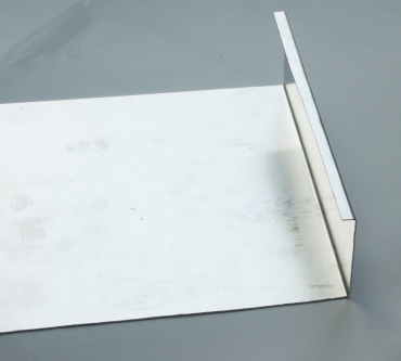
Just bend the aluminum twice. This is easy to do even without
professional equipment.
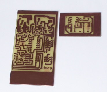
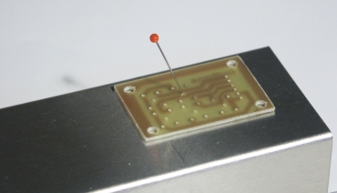
The two printed circuit boards. The smaller one is for the keyboard.
Mark the positions of the push buttons on the case before you
solder the buttons onto the board. This makes it easy to drill the
holes at the right position.
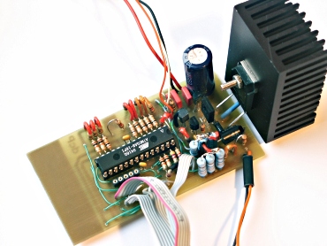
The circuit. Very small, feature rich and powerful.
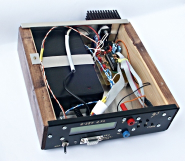
The final powersupply.
Have fun! ... and there will be more fun because this hardware can do much
more...
References/Download
- Download page for this article (updates
and corrections will also be available from here).
- How to program the atmega8 with gcc: November2004 article
352
- Datasheet for the Atmega8: go to http://www.atmel.com/
and select products->Microcontrollers ->AVR-8 bit
RISC->Documentation->datasheets
(local copy, pdf,
2479982 bytes)
- Tuxgraphics electronics section, a collection of all articles in this series.
- Tuxgraphics
online shop, microcontroller section, You can order all parts (transistors,
passive components, LCD display, PCB, microcontroller, ...) from here.
Talkback form for this article
Every article has its own talkback page. On this page you can submit a comment or look at comments from other readers:
2006-02-25, generated by lfparser version 2.52