|
|
|
| This document is available in: English Deutsch Francais Turkce |
![[Photo of the Author]](../../common/images/article300/BobSmith2.jpg)
by Bob Smith <bob(Q)linuxtoys.org> About the author: Bob is an electronics hobbyist and Linux programmer. You can find his latest project at www.linuxappliancedesign.com and his homepage at www.linuxtoys.org. Content: |
A 1 Bit Data Scope
Abstract:
The 1 Bit Data Scope captures one bit of data at a rate of
46080 (or 92160) samples per second and encodes the data into a
stream of RS-232 characters which can be read at 57.6 (or
115.2) kilobaud. The Data Scope is a fairly simple construction
project which uses six low cost IC's.
|
The problem is that we need to store the input samples while
we are sending the start and stop bits. The following diagram
illustrates the problem. 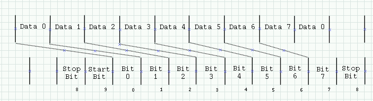
During bits 0, 1, 2, and 3, we want the data delayed by two
data clocks, so we select Q(B) from the 4015 shift register.
During bits 4, 5, 6, and 7, we want the data delayed by one
data clock, so we select Q(A) from the shift register. During
the stop and start bits (bits 8 and 9) we want a zero and one,
so we select Q(0) of the bit counter.

The schematic capture was done with a very nice package called "EAGLE" available from Cadsoft. The schematic file for the above circuit is available as 1bitla.sch.gz.
To run the circuit at 115.2 kHz, use the Q(1) and Q(4) outputs of the 4024 instead of the Q(2) and Q(5) outputs. Other baud rates are possible by using a different value for the crystal or by replacing the crystal oscillator with an RC oscillator.
You may find that the crystal oscillator draws less power than an RC circuit at the same frequency. To conserve power be sure to ground the unused inputs of the 4049 hex inverter.
A better input buffer might be to use the second op-amp in the TL082. You can use a resistor divider attached to one op-amp input and use the other input for the data in. This lets you control the threshold very accurately and presents a very high impedance to the device under test.
RTS provide power (Vcc) for the rest of circuit. In the prototype Vcc was about 7 volts. Your voltage for Vcc may vary depending on the computer's RS-232 interface. The software driving the Data Scope must set both DTR and RTS high.
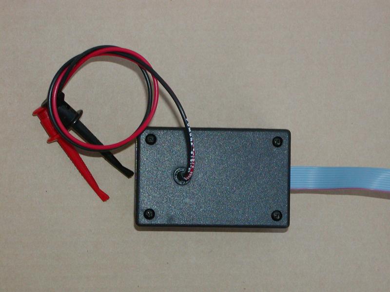
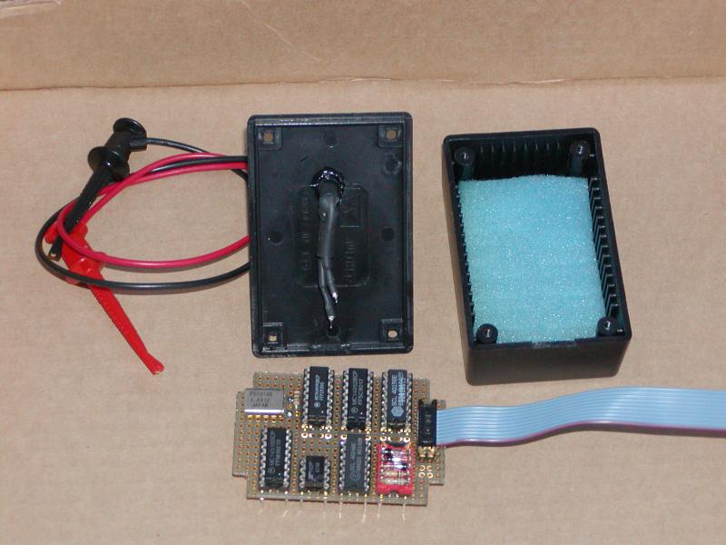
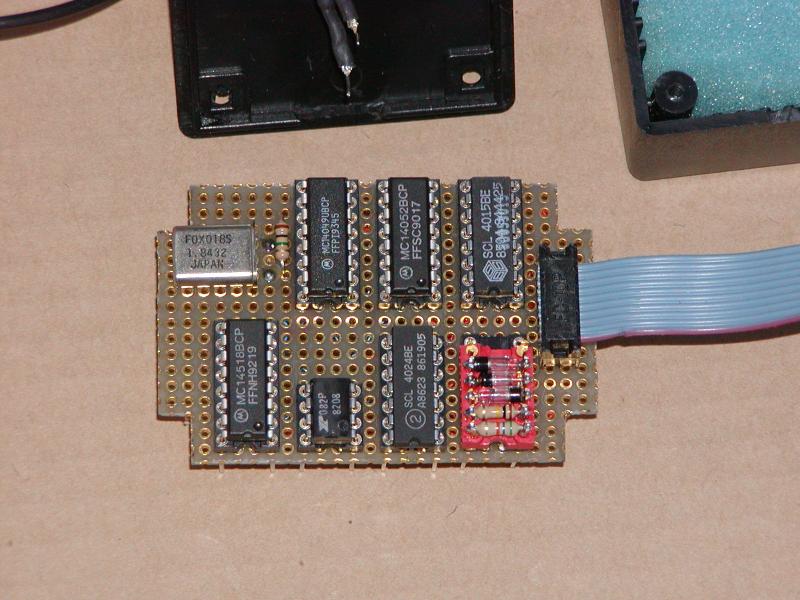
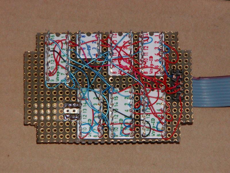
Here are some photos to show you one approach to the
construction.
|
|
||
|---|---|---|
| -r | -c | -t |
| 03 e3 ff 03 e3 ff 03 e3 ff 03 e3 ff 03 e3 ff 03 e3 ff 03 e3 ff 03 e3 ff 03 e3 ff 03 e3 ff 03 e3 ff 03 e3 |
0, 0 1, 5 0, 3 1, 10 0, 6 1, 5 0, 3 1, 10 0, 6 1, 5 0, 3 1, 10 0, 6 1, 5 0, 3 1, 10 0, 6 1, 5 0, 3 1, 10 0, 6 1, 5 0, 3 1, 10 0, 6 1, 5 0, 3 1, 10 |
0, 0.000000 1, 0.000065 0, 0.000065 1, 0.000217 0, 0.000130 1, 0.000109 0, 0.000065 1, 0.000217 0, 0.000130 1, 0.000109 0, 0.000065 1, 0.000217 0, 0.000130 1, 0.000109 0, 0.000065 1, 0.000217 0, 0.000130 1, 0.000109 0, 0.000065 1, 0.000217 0, 0.000130 1, 0.000109 0, 0.000065 1, 0.000217 0, 0.000130 1, 0.000109 0, 0.000065 1, 0.000217 |
The simple program here (1bitla.c) captures the serial data and can output the data in three formats. The first format is the raw data, displayed one byte per line with a two character hex display. Note that the program inverts the data before display, and that the data is sent MSB first. Raw output is invoked with the -r command line option. The second format is a value (0 or 1) followed by a count of how many one bit samples had that value. The value/count output is invoked with the -c option. The third output format is a value (0 or 1) followed by the number of seconds the input had that value. The resolution at 46080 kHz is 21.7 microseconds. The value/time output is invoked with the -t option.
The program is invoked as
1bitla [option] serial_port
where option can be -r, -c, or -t. The default is value/count
(-c).
The design of the program is fairly simple. We process the command line options, open the serial port, and loop forever reading and displaying bytes. Since we are not doing any background processing we use a blocking read.
You may be satisfied with just displaying the samples to the
console or redirecting them into a file for later processing,
or you might want to perform a true "logic analysis" on the
data by building a state machine to process the samples.
Example state machines might include decoding commands sent
from an infrared remote control, or decoding the position of a
radio controlled pulse width modulated output.
|
|
Webpages maintained by the LinuxFocus Editor team
© Bob Smith, FDL LinuxFocus.org |
Translation information:
|
2003-07-01, generated by lfparser version 2.38